
|
 03 January 2017, 04:45
|
#1 |
|
Registered User
Join Date: Dec 2016
Location: Australia
Posts: 113
|
A500 trapdoor memory: free design
Hi EAB,
A couple of months ago I picked up a cheap A500 from a local ad. It's the first one I've had since the 1990s, so it's quite nostalgic to look at, handle, power up. When I opened up the trapdoor of this unit, I fully expected to find a battery damaged A501. But, shock, empty! Nothing in there. So maybe I can find some suitable RAMs from some of my old PC SIMM sticks? These look pretty good. A quick look at the data sheet shows they are 16-bits wide, perfect for a A500.  Break out the heat gun / paint stripper:  It comes right off, easy  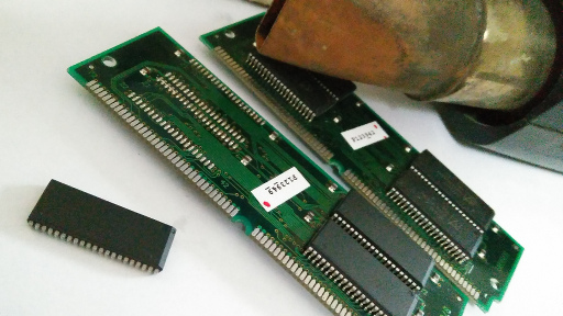 Fast forward some playing with a PCB CAD program. This is all you need:   Done! Ready for a fitment test  Damn! Look how old my A500 is, very early serial number.  It fits very well. Ready for the smoke test:  It works! Never doubted it. Fun to recycle some old scrap RAM chips.  Now I have a few spare boards. If somebody wants one for personal use (without parts) I'm happy to send it via letter post for AU$3 in Australia or AU$5 world wide. A small donation above that is welcome but not necessary. The memory chips are easy to find on old EDO memory sticks, and the capacitor I can include if you don't have it. EDIT: Demand is too high, so I bumped the price to $5, I need to buy envelopes EDIT: More RAM details: The memory you are searching for is 72-pin, so try that as a search term on Ebay. Technically, the chips are called SOJ42, 1M x 16. You can identify them visually, they are the bigger/longer chips. If you count 21 pins on one side (42 total), it's a winner. They are pretty cheap and abundant, I've seen some advertised for $2 for a few SIMMs that gets you about 8 chips! So what are those pads for another two memory chips for? Good question! They are untested, but in theory it's for: - 1.0 MB in A500+ plus to give you a full 2MB chip RAM. - 1.5 MB in a normal A500 with a gary adapter. See post #60 about buying a board. //Pete. Last edited by PeteAU; 05 March 2017 at 10:40. |

|
|
03 January 2017, 04:45
|
#2 |
|
Registered User
Join Date: Dec 2016
Location: Australia
Posts: 113
|
PCB design files
Rev B6: Eagle schematic and board: http://pibus.info/amiga/a501/miniA501b6.zip
Gerber files (for production) http://pibus.info/amiga/a501/miniA501b6_gerbers.zip Changes: - Added a jumper for RTC enable. - Added a footprint for SMD RTC chip, so you can populate either one. - Made jumper drills larger (0.8->0.9mm) per Mathesar's complaint. - Gary adapter by Mathesar with flipflops for BLIT. - Corrected JP4 error on gary adapter. - Improved decoupling caps positioning. Rev C6: Gerber files (for production) http://pibus.info/amiga/a501/miniA50...40_gerbers.zip Changes: - For different memory: SOJ40. Don't consider this board "better" or "newer", it's just for different memory types. Apparently you can find some SOJ40 memory on old AGP video cards. If you've never had PCBs made, it's dead easy: - Visit your favourite cheap Chinese board house: Elecrow, iteadstudio, seeedstudio etc e.g. https://www.elecrow.com/pcb-manufacturing.html - Upload the gerbers ZIP file. - Select 100x100mm, HASL and 1.2mm thickness. Done! Parts List: - For the main board: http://eab.abime.net/showpost.php?p=...9&postcount=62 - For the real-time-clock: http://eab.abime.net/showpost.php?p=...9&postcount=14 Last edited by PeteAU; 06 May 2020 at 05:46. |
|
|
|
03 January 2017, 07:00
|
#3 |
|
Unregistered User
Join Date: Sep 2012
Location: Copenhagen / DK
Age: 43
Posts: 4,190
|
Looks great - I would love to have one. I should have the components available and I would try to make a 1 MB one for a 500+.
|
|
|
|
03 January 2017, 07:41
|
#4 |
|
Registered User
Join Date: May 2015
Location: Somewhere in Time
Posts: 490
|
Wow, that pcb makes my 512k slow ram look.. terrible. I think it was made locally in 1987 or something.. and sure looks the part (i.e. ugly). I would love to have one of the boards and the capacitor. Finding the EDO chips won't be easy over here but I'll try. (Not that I have any idea how to solder the ram chips onto the board, but we do what we must because we can..) Please PM me your paypal details so I can send you the postage cost
Out of curiosity, what happens if I make a 1.5MB card and add it to a Rev6 A500? |
|
|
|
03 January 2017, 07:54
|
#5 | |
|
-
Join Date: Jul 2003
Location: Helsinki / Finland
Age: 43
Posts: 9,861
|
Quote:
|
|
|
|
|
03 January 2017, 08:02
|
#6 | |
|
Registered User
Join Date: May 2015
Location: Somewhere in Time
Posts: 490
|
Quote:

|
|
|
|
|
03 January 2017, 08:39
|
#7 | ||
|
Registered User
Join Date: Dec 2016
Location: Australia
Posts: 113
|
Quote:
Quote:
|
||
|
|
|
03 January 2017, 14:37
|
#8 |
|
-
Join Date: Jul 2003
Location: Helsinki / Finland
Age: 43
Posts: 9,861
|
It is relatively simple to convert this to an A500+ 1MB expansion, but you will need to solder a few jump wires to hook up the RAS + CAS signals to the other mem bank and to the motherboard connector. See elsewhere in this subforum for information on how to do this, someone converted a 512k A500 expansion to 1M some months ago.
Ah well, here you go: http://eab.abime.net/showthread.php?t=83121 It doesn't spoon feed you, but it has the info you need. Congrats PeteAU on a nice design, I like how you made it configurable. Did you check http://eab.abime.net/showthread.php?t=49965 for info on the gary adapter logic? I'm at work, so I didn't take a look at how you did yours yet. :-D Last edited by Jope; 03 January 2017 at 14:47. |
|
|
|
03 January 2017, 15:09
|
#9 |
|
Registered User
Join Date: May 2015
Location: Somewhere in Time
Posts: 490
|
Could any of you fine gents let me know what kind of SIMM I should hunt for chips to solder onto this? Do I want 512Kx16-bit? Would 1Mx16-bit work?
|
|
|
|
03 January 2017, 15:42
|
#10 | |
|
Registered User
Join Date: Dec 2016
Location: Australia
Posts: 113
|
Yeah, I just looked at the 500+ schematic, I think it won't need any wires for 1MB, just the right jumper settings.
Jope, did you already make a similar board? For the Gary adaptor, I tried to cater for two scenarios, the first one is easy, the second one more challenging with just NAND gates: Scenario#1: 0.5chip 1.5slow - only 2 wires from Gary to trapdoor's 74139. Chip 000000 - 07FFFF (internal, RAS0) Slow C00000 - C7FFFF (trapdoor, RAS1, A20:A19 is 00) Slow C80000 - CFFFFF (trapdoor, RAS1, A20:A19 is 01) Slow D00000 - D7FFFF (trapdoor, RAS1, A20:A19 is 10) Scenario#2: 1.0chip 0.5/1.0 slow - this requires an extra wire to JP2 (Agnus A19) to force RAS1 at $C0. I have chosen to use A23 instead. Chip 000000 - 07FFFF (internal, RAS0) Chip 080000 - 0FFFFF (trapdoor, RAS1, A23:A19 is 01) Slow C00000 - C7FFFF (trapdoor, RAS faulty, A23:A19 is 10) Slow C80000 - CFFFFF (trapdoor, RAS1, A23:A19 is 11) My suspicion is, in scenario #2, the A500 will normally assert a RAS0 for $C0, which needs to be overridden. But I'm not sure, I can't see Agnus's guts/logic. Does Agnus use A19 (pin 59) to decide which RAS? Besides that, the adaptor also changes Gary's (or actually Agnus's) RGAEN and RAMEN signals in this way: http://pibus.info/amiga/a501/1m5_gary2.png I think I achieved _all_ of the above with just two 74F00s. Maybe. Thanks for the links Jope, I'll have a read of those threads later. Anyway... I tried to buy a A500+ motherboard on ebay.co.uk a few times, but you Brits don't want to ship them to AU for some reason. Are you hording them? Quote:
Last edited by PeteAU; 04 January 2017 at 00:07. Reason: Jope mixed up authors |
|
|
|
|
03 January 2017, 19:45
|
#11 |
|
Registered User
Join Date: Aug 2016
Location: Cresco, PA, USA
Age: 53
Posts: 1,126
|
If there are any left, I'd like a board or two.
|
|
|
|
03 January 2017, 20:47
|
#12 |
|
Registered User
Join Date: Dec 2016
Location: dronfield
Posts: 32
|
Looks great, been on the lookout for an expansion for my A500 plus. Sent a message.
|
|
|
|
04 January 2017, 00:45
|
#13 |
|
Registered User
Join Date: Feb 2016
Location: bolton
Posts: 145
|
hi have you got a revision B schematic for the 1.5mb version?
|
|
|
|
04 January 2017, 00:58
|
#14 |
|
Registered User
Join Date: Dec 2016
Location: Australia
Posts: 113
|
I populated the real time clock and with a bit of minimal testing, it appears to work
The clock is completely optional of course, you don't need to bother with it if you don't want one.The parts list for RTC: U5 or U6: RTC62421/RTC72421/RTC62423/RTC72423 C10 or R7: 47K-100K 0805 resistor (yes a resistor!) C12: 100nF 0805 capacitor C13 or C19: >=2.2μF >=10V 0805 or 1206 tantalum R1, R2, R3: 10K 0805 resistor R4, R5: 220-470 0805 resistor D1: BAT721C or BAT54C diode Battery Holder: Some cheap ebay one. Last edited by PeteAU; 23 September 2017 at 01:54. |
|
|
|
04 January 2017, 01:16
|
#15 | |
|
Registered User
Join Date: Dec 2016
Location: Australia
Posts: 113
|
Quote:
Here's a alpha/beta/notready. I'm sure it's fine for 0.5meg chip ram system, but you tell me if it'd work on a 1meg. |
|
|
|
|
04 January 2017, 06:18
|
#16 | |
|
Registered User
Join Date: May 2015
Location: Somewhere in Time
Posts: 490
|
Quote:
1Mx16 it is)EDIT2: Ended up buying some Alliance AS4C1M16E5-60JC from Aliexpress.. 1Mx16 5V DRAM EDO chips.. Hope I'm doing it right guys.. Last edited by appiah4; 04 January 2017 at 15:23. |
|
|
|
|
04 January 2017, 21:51
|
#17 |
|
Registered User
Join Date: Dec 2016
Location: dronfield
Posts: 32
|
Thanks, sent money through paypal.
I know its un-tested, but in theory what jumpers do I need to join for 1mb chip expansion on an A500+? I guess i'll try it as 512kb first, one step at a time. Thanks again |
|
|
|
05 January 2017, 03:27
|
#18 | |
|
Registered User
Join Date: Dec 2016
Location: Australia
Posts: 113
|
Quote:
Last edited by PeteAU; 17 January 2017 at 00:17. |
|
|
|
|
07 January 2017, 16:23
|
#19 |
|
Posts: n/a
|
From the A500+ service manual (talking about the 8375)
"In the 1 meg configuration, A19 is still used to determine the RAS line to be asserted. If A19 is low RAS0* is active and if high RAS1* is active" I suspect the predecessors of 8375 work the same way. In (unmodified) R5 and R6A A500s CPU's A23 is routed to Agnus' A19 via JP2. In (unmodified) R8a A500+s CPU's A19 is routed to Agnus' A19 via JP2. |
|
07 January 2017, 16:40
|
#20 |
|
Registered User
Join Date: Feb 2012
Location: #DrainTheSwamp
Posts: 4,545
|
can you tell me where i may find this memory test tool/module?
|
|
|
| Currently Active Users Viewing This Thread: 1 (0 members and 1 guests) | |
| Thread Tools | |
 Similar Threads
|
||||
| Thread | Thread Starter | Forum | Replies | Last Post |
| Modern Trapdoor RAM killed my A500 | Silwuff | New to Emulation or Amiga scene | 20 | 10 January 2021 15:36 |
| Homemade A500 trapdoor expansion? | cabal | Hardware mods | 5 | 01 December 2014 21:44 |
| WTB: two(2) A500 trapdoor slot covers | papa_november | MarketPlace | 0 | 25 December 2008 09:17 |
| Trapdoor expansion options for A500 | Impakt | support.Hardware | 7 | 20 March 2008 06:05 |
| A500 Plus Trapdoor Expansion | TheCorfiot | support.Hardware | 10 | 14 March 2008 16:42 |
|
|


