
|
 28 August 2008, 23:44
|
#1 |
|
Vegetable Lasagna
Join Date: Mar 2007
Location: Toronto, CANADA
Age: 54
Posts: 711
|
I need some (more) help from one of our resident hardware experts...
 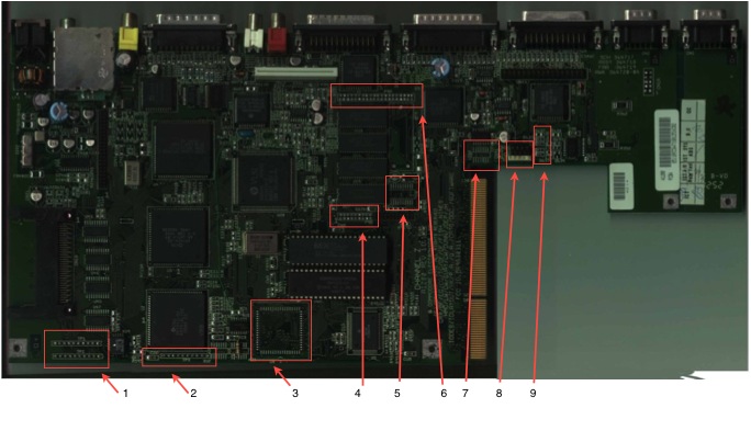 I'm trying to figure out exactly what the numbered spots/solder points are for. With #8 I know that the bottom set of pins are for the case LEDs so I'm wondering about the set of pins above it (I worried that making the box smaller would lead to confusion). I suspect that this information might be available on a schematic but I don't have nearly enough knowledge to figure one of those out. Any answers would be more appreciated. Thanks in advance. 
|

|
|
28 August 2008, 23:54
|
#2 |
|
Registered User

Join Date: Nov 2006
Location: Amigaville
Age: 46
Posts: 3,338
|
I'm pretty certain number 3 was for a maths co-processor...
|
|
|
|
29 August 2008, 00:09
|
#3 |
|
Registered User
Join Date: Dec 2007
Location: Oooh what a feeling yeaaah dancing on the ceiling
Posts: 314
|
I think #4 is "remainder" clock-port connector points.
#8 has my floppy drive plugged in above the case leds. Last edited by meega; 29 August 2008 at 00:19. |
|
|
|
29 August 2008, 00:28
|
#4 |
|
Registered User
Join Date: Nov 2006
Location: Amigaville
Age: 46
Posts: 3,338
|
no 5. is for a Real time clock
no. 6 EDGE-90 Memory Bus Expansion(very OLD! model) and Real-Time Clock/Calendar no 3. is deffo the fpu - 68881 68-pin PLCC I'm getting info from here although it's not fully complete... http://www.amigahistory.co.uk/a1200info1.txt |
|
|
|
29 August 2008, 00:28
|
#5 | |||
|
Vegetable Lasagna
Join Date: Mar 2007
Location: Toronto, CANADA
Age: 54
Posts: 711
|
Quote:
Quote:
Quote:

|
|||
|
|
|
29 August 2008, 03:37
|
#6 |
|
Ya' like it Retr0?
Join Date: Jul 2005
Location: United Kingdom
Age: 49
Posts: 9,768
|
1. Test Point [TP 1 and 2]
2. Test Point [TP 3] 3. FPU 68882 4. Clock Port Header 5. Clock chip 6. DRAM Port 7. defunct component 8. LED/Power Header 9. Activity Coupling 4. This is infact Clock Port 2  6. This was intended as the a chip ram expansion as the A1200 was gonna have 1MB) 9. Here is the Activity Coupling for the LED's, you can add a small trimpot to the arrary and give yourself PCMCIA Activity LED 
|
|
|
|
29 August 2008, 05:09
|
#7 | |
|
Vegetable Lasagna
Join Date: Mar 2007
Location: Toronto, CANADA
Age: 54
Posts: 711
|
Quote:
|
|
|
|
|
29 August 2008, 05:35
|
#8 |
|
I hate potatos and shirts
Join Date: Oct 2007
Location: Sao Leopoldo / Brazil
Age: 58
Posts: 3,482
  |
Maybe. Nobody even try. Neither the soldered FPU, nor the PCMCIA activity LED (wait! this was made!). The problem is the shape of the clockport boards, all intended to fit just on the right cp.
|
|
|
|
30 August 2008, 12:16
|
#9 | |
|
Hamster tamer
Join Date: Apr 2007
Location: Out in the woods
Posts: 122
|
Quote:
Edit: BTW, both P9B+P9A were the connections for the 1MB chip ram expansion. When they decided to ship with 2MB, they removed all the pins for the expansion except for those needed for an RTC.. so the right side of P9B got known as the 'clock port' |
|
|
|
| Currently Active Users Viewing This Thread: 1 (0 members and 1 guests) | |
| Thread Tools | |
 Similar Threads
|
||||
| Thread | Thread Starter | Forum | Replies | Last Post |
| LCDaemon - any experts here? | spotUP | Amiga scene | 0 | 25 June 2013 18:59 |
| Need hardware experts help | AmigaDave | Hardware mods | 0 | 16 October 2011 05:55 |
| Calling it a day... | killergorilla | project.Killergorilla's WHD packs | 57 | 28 March 2011 06:48 |
| Calling All Contributors! | fiath | project.SPS (was CAPS) | 9 | 28 October 2010 12:22 |
| Protection experts out there? | NOB | support.Games | 5 | 13 September 2005 17:38 |
|
|


