
|
 25 March 2020, 17:55
|
#21 |
|
Natteravn
Join Date: Nov 2009
Location: Herford / Germany
Posts: 2,496
|
@Bruce: You really have to relax! What's the reason for your harsh tone in most discussions? Did Saimo do anything to you? Is it your ROM code he is talking about?

|

|
|
27 March 2020, 00:46
|
#22 |
|
Registered User
Join Date: Aug 2010
Location: Italy
Posts: 787
|
Back from a little break (dedicated, among other things, to
[ Show youtube player ], which provided me with some relaxing distraction from this matter).
I looked again and at a bit further into the log... Code:
SCL SDA operation cycle ----------------------------------------------------------------------------- * INITIALIZE 28-077 [98 062-111]: Direction write: 00->c0 o o 28-077 [98 062-111]: Data write: c0->c0 (c0) 1 1 * START 28-077 [98 108-111]: I2C START 28-077 [98 108-111]: Data write: c0->80 (80) 1 0 start * ADDRESS MEMORY (for write) 28-077 [98 167-111]: Data write: 80->00 (00) 0 0 1v 28-077 [98 221-111]: Data write: 00->40 (40) 0 1 28-077 [98 041-112]: Data write: 40->c0 (c0) 1 1 send 1 1^ 28-077 [98 074-112]: Data write: c0->40 (40) 0 1 28-077 [98 104-112]: Data write: 40->00 (00) 0 0 28-077 [98 134-112]: Data write: 00->80 (80) 1 0 send 0 2^ 28-077 [98 154-112]: Data write: 80->00 (00) 0 0 28-077 [98 188-112]: Data write: 00->40 (40) 0 1 28-077 [98 219-112]: Data write: 40->c0 (c0) 1 1 send 1 3^ 28-077 [98 012-113]: Data write: c0->40 (40) 0 1 28-077 [98 046-113]: Data write: 40->00 (00) 0 0 28-077 [98 073-113]: Data write: 00->80 (80) 1 0 send 0 4^ 28-077 [98 102-113]: Data write: 80->00 (00) 0 0 28-077 [98 132-113]: Data write: 00->00 (00) 0 0 28-077 [98 162-113]: Data write: 00->80 (80) 1 0 send 0 5^ 28-077 [98 187-113]: Data write: 80->00 (00) 0 0 28-077 [98 217-113]: Data write: 00->00 (00) 0 0 28-077 [98 020-114]: Data write: 00->80 (80) 1 0 send 0 6^ 28-077 [98 040-114]: Data write: 80->00 (00) 0 0 28-077 [98 074-114]: Data write: 00->00 (00) 0 0 28-077 [98 101-114]: Data write: 00->80 (80) 1 0 send 0 7^ 28-077 [98 130-114]: Data write: 80->00 (00) 0 0 28-077 [98 160-114]: Data write: 00->00 (00) 0 0 28-077 [98 190-114]: Data write: 00->80 (80) 1 0 send 0 8^ * GET ACK 28-077 [98 218-114]: Direction write: c0->80 o i 28-077 [98 218-114]: Data write: 80->00 (40) 0 * 9v 28-077 [98 041-115]: I2C device address 0xa0 28-077 [98 041-115]: Data write: 40->80 (c0) 1 * 9^ 28-077 [98 074-115]: Direction read: 80 o i 28-077 [98 074-115]: Data read: 00 * 0 get ACK * ??? 28-077 [98 082-115]: Data write: c0->00 (40) 0 * ? 10v 28-077 [98 093-115]: Data write: 40->00 (40) 0 * ? * ADDRESS OFFSET 28-077 [98 128-115]: Direction write: 80->c0 o o 28-077 [98 128-115]: Data write: 40->00 (00) 0 0 28-077 [98 165-115]: Data write: 00->80 (80) 1 0 10^ 28-077 [98 198-115]: Data write: 80->00 (00) 0 0 28-078 [98 005-116]: Data write: 00->00 (00) 0 0 28-078 [98 032-116]: Data write: 00->80 (80) 1 0 11 28-078 [98 061-116]: Data write: 80->00 (00) 0 0 28-078 [98 091-116]: Data write: 00->00 (00) 0 0 28-078 [98 121-116]: Data write: 00->80 (80) 1 0 12 28-078 [98 146-116]: Data write: 80->00 (00) 0 0 28-078 [98 176-116]: Data write: 00->00 (00) 0 0 28-078 [98 206-116]: Data write: 00->80 (80) 1 0 13 28-078 [98 226-116]: Data write: 80->00 (00) 0 0 28-078 [98 033-117]: Data write: 00->00 (00) 0 0 28-078 [98 060-117]: Data write: 00->80 (80) 1 0 14 28-078 [98 089-117]: Data write: 80->00 (00) 0 0 28-078 [98 119-117]: Data write: 00->00 (00) 0 0 28-078 [98 149-117]: Data write: 00->80 (80) 1 0 15 28-078 [98 174-117]: Data write: 80->00 (00) 0 0 28-078 [98 204-117]: Data write: 00->00 (00) 0 0 28-078 [98 007-118]: Data write: 00->80 (80) 1 0 16 28-078 [98 027-118]: Data write: 80->00 (00) 0 0 28-078 [98 061-118]: Data write: 00->00 (00) 0 0 28-078 [98 088-118]: Data write: 00->80 (80) 1 0 17 28-078 [98 170-118]: I2C device address 0x00 (Address 0000) * GET ACK 28-078 [98 119-118]: Direction write: c0->80 o i 28-078 [98 119-118]: Data write: 80->00 (40) 0 0 28-078 [98 170-118]: Data write: 40->80 (c0) 1 0 18 28-078 [98 207-118]: Direction read: 80 28-078 [98 207-118]: Data read: 00 0 0 get ACK * RESTART 28-078 [98 211-118]: Data write: c0->00 (40) 0 * 19v 28-078 [98 001-119]: Direction write: 80->c0 o o 28-078 [98 001-119]: Data write: 40->c0 (c0) 1 1 19^ extra cycle 28-078 [98 047-119]: Data write: c0->80 (80) 1 0 28-078 [98 047-119]: I2C START * ADDRESS MEMORY (for read) 28-078 [98 101-119]: Data write: 80->00 (00) 0 0 20v 28-078 [98 135-119]: Data write: 00->40 (40) 0 1 28-078 [98 182-119]: Data write: 40->c0 (c0) 1 1 20^ 28-078 [98 215-119]: Data write: c0->40 (40) 0 1 21v 28-078 [98 018-120]: Data write: 40->00 (00) 0 0 28-078 [98 048-120]: Data write: 00->80 (80) 1 0 21^ 28-078 [98 068-120]: Data write: 80->00 (00) 0 0 22v 28-079 [98 102-120]: Data write: 00->40 (40) 0 1 28-079 [98 133-120]: Data write: 40->c0 (c0) 1 1 22^ 28-079 [98 153-120]: Data write: c0->40 (40) 0 1 23v 28-079 [98 187-120]: Data write: 40->00 (00) 0 0 28-079 [98 214-120]: Data write: 00->80 (80) 1 0 23^ 28-079 [98 016-121]: Data write: 80->00 (00) 0 0 24v 28-079 [98 046-121]: Data write: 00->00 (00) 0 0 28-079 [98 076-121]: Data write: 00->80 (80) 1 0 24^ 28-079 [98 101-121]: Data write: 80->00 (00) 0 0 25v 28-079 [98 131-121]: Data write: 00->00 (00) 0 0 28-079 [98 161-121]: Data write: 00->80 (80) 1 0 25^ 28-079 [98 181-121]: Data write: 80->00 (00) 0 0 26v 28-079 [98 215-121]: Data write: 00->00 (00) 0 0 28-079 [98 015-122]: Data write: 00->80 (80) 1 0 26^ 28-079 [98 044-122]: Data write: 80->00 (00) 0 0 27v 28-079 [98 078-122]: Data write: 00->40 (40) 0 1 28-079 [98 105-122]: Data write: 40->c0 (c0) 1 1 27^ * GET ACK 28-079 [98 137-122]: Direction write: c0->80 o i 28-079 [98 137-122]: Data write: c0->40 (40) 0 * 28v 28-079 [98 188-122]: Data write: 40->c0 (c0) 1 * 28^ 28-079 [98 224-122]: Direction read: 80 28-079 [98 224-122]: Data read: 00 0 0 get ACK * ??? 28-079 [98 001-123]: Data write: c0->00 (40) 0 * 29v 28-079 [98 019-123]: Data write: 40->00 (40) 0 * 28-079 [98 021-123]: Data write: 40->00 (40) 0 * * READ BYTE 0 28-079 [98 059-123]: I2C RX byte 0000 0x00 28-079 [98 059-123]: Data write: 40->80 (c0) 1 * 29^ 28-079 [98 092-123]: Direction read: 80 28-079 [98 092-123]: Data read: 00 28-079 [98 099-123]: Data write: c0->00 (40) 28-079 [98 122-123]: Data write: 40->80 (c0) 31^ 28-079 [98 143-123]: Direction read: 80 28-079 [98 143-123]: Data read: 00 28-079 [98 147-123]: Data write: c0->00 (40) 28-079 [98 172-123]: Data write: 40->80 (c0) 32^ 28-079 [98 192-123]: Direction read: 80 28-079 [98 192-123]: Data read: 00 28-079 [98 196-123]: Data write: c0->00 (40) 28-079 [98 217-123]: Data write: 40->80 (c0) 33^ 28-079 [98 011-124]: Direction read: 80 28-079 [98 011-124]: Data read: 00 28-079 [98 015-124]: Data write: c0->00 (40) 28-079 [98 040-124]: Data write: 40->80 (c0) 34^ 28-080 [98 060-124]: Direction read: 80 28-080 [98 060-124]: Data read: 00 28-080 [98 064-124]: Data write: c0->00 (40) 28-080 [98 085-124]: Data write: 40->80 (c0) 35^ 28-080 [98 106-124]: Direction read: 80 28-080 [98 106-124]: Data read: 00 28-080 [98 110-124]: Data write: c0->00 (40) 28-080 [98 135-124]: Data write: 40->80 (c0) 36^ 28-080 [98 155-124]: Direction read: 80 28-080 [98 155-124]: Data read: 00 28-080 [98 159-124]: Data write: c0->00 (40) 28-080 [98 180-124]: Data write: 40->80 (c0) 37^ 28-080 [98 201-124]: Direction read: 80 28-080 [98 201-124]: Data read: 00 * SEND ACK 28-080 [98 208-124]: Data write: c0->00 (40) 0 * 38v 28-080 [98 048-125]: Direction write: 80->c0 o o 28-080 [98 048-125]: Data write: 40->00 (00) 0 0 28-080 [98 085-125]: I2C ACKED 28-080 [98 085-125]: Data write: 00->80 (80) 1 0 38^ * ??? 28-080 [98 124-125]: Data write: 80->00 (00) 0 0 39v 28-080 [98 135-125]: Direction write: c0->80 o i 28-080 [98 135-125]: Data write: 00->00 (40) 0 * 28-080 [98 135-125]: Data write: 40->00 (40) 0 * * READ BYTE 1 28-080 [98 163-125]: I2C RX byte 0001 0x56 28-080 [98 163-125]: Data write: 40->80 (c0) 1 * 39^ 28-080 [98 184-125]: Direction read: 80 28-080 [98 184-125]: Data read: 00 28-080 [98 188-125]: Data write: c0->00 (40) 28-080 [98 213-125]: Data write: 40->80 (c0) 28-080 [98 006-126]: Direction read: 80 28-080 [98 006-126]: Data read: c0 28-080 [98 010-126]: Data write: c0->00 (40) 28-080 [98 032-126]: Data write: 40->80 (c0) 28-080 [98 057-126]: Direction read: 80 28-080 [98 057-126]: Data read: 00 28-080 [98 065-126]: Data write: c0->00 (40) 28-080 [98 086-126]: Data write: 40->80 (c0) 28-080 [98 107-126]: Direction read: 80 28-080 [98 107-126]: Data read: c0 28-080 [98 111-126]: Data write: c0->00 (40) 28-080 [98 136-126]: Data write: 40->80 (c0) 28-080 [98 157-126]: Direction read: 80 28-080 [98 157-126]: Data read: 00 28-080 [98 161-126]: Data write: c0->00 (40) 28-080 [98 186-126]: Data write: 40->80 (c0) 28-080 [98 206-126]: Direction read: 80 28-080 [98 206-126]: Data read: c0 28-080 [98 210-126]: Data write: c0->00 (40) 28-080 [98 005-127]: Data write: 40->80 (c0) 28-080 [98 030-127]: Direction read: 80 28-080 [98 030-127]: Data read: c0 28-081 [98 038-127]: Data write: c0->00 (40) 28-081 [98 059-127]: Data write: 40->80 (c0) 28-081 [98 080-127]: Direction read: 80 28-081 [98 080-127]: Data read: 00 28-081 [98 084-127]: Data write: c0->00 (40) 28-081 [98 147-127]: Direction write: 80->c0 28-081 [98 147-127]: Data write: 40->00 (00) 28-081 [98 175-127]: I2C ACKED (Continued in the next post.) |
|
|
|
27 March 2020, 00:56
|
#23 |
|
Registered User
Join Date: Aug 2010
Location: Italy
Posts: 787
|
(Continued.)
I felt that looking at the log wasn't sufficient to fully understand the logic (and check the timings), so I decided to challenge my sanity and follow the execution from the UAE monitor (for those who find this strange, again, it's a limitation of mine). I couldn't take much, but something came out of it... Code:
*** initialization Memwatch 1: break at 00B80030.L W C000C000 PC=00E61A12 CPUDW (000) hh oo 00E61A12 2a85 MOVE.L D5,(A5) [c000c000] 00E61A14 4a39 00bf e001 TST.B $00bfe001 00E61A1A 4a39 00bf e001 TST.B $00bfe001 00E61A20 4a39 00bf e001 TST.B $00bfe001 00E61A26 4a39 00bf e001 TST.B $00bfe001 00E61A2C 0285 bfff ffff AND.L #$bfffffff,D5 *** START condition Memwatch 1: break at 00B80030.L W 8000C000 PC=00E61A32 CPUDW (000) hl oo 00E61A32 2a85 MOVE.L D5,(A5) [0000c000] 8000C000 00E61A34 4a39 00bf e001 TST.B $00bfe001 00E61A3A 4a39 00bf e001 TST.B $00bfe001 00E61A40 4a39 00bf e001 TST.B $00bfe001 00E61A46 4e75 RTS *** send byte (address memory) Memwatch 1: break at 00B80030.L W 0000C000 PC=00E61ABC CPUDW (000) ll oo v 00E61AB4 7207 MOVE.L #$07,D1 00E61AB6 0285 7fff ffff AND.L #$7fffffff,D5 00E61ABC 2a85 MOVE.L D5,(A5) [0000c000] 0000C000 00E61ABE 4a39 00bf e001 TST.B $00bfe001 00E61AC4 4a39 00bf e001 TST.B $00bfe001 00E61ACA 4a39 00bf e001 TST.B $00bfe001 00E61AD0 4a39 00bf e001 TST.B $00bfe001 00E61AD6 0285 bfff ffff AND.L #$bfffffff,D5 Memwatch 1: break at 00B80030.L W 4000C000 PC=00E61AEC CPUDW (000) lh oo 00E61ADC 0085 0000 4000 OR.L #$00004000,D5 00E61AE2 e388 LSL.L #$01,D0 00E61AE4 6406 BCC.B #$06 == $00e61aec (T) 00E61AE6 0085 4000 0000 OR.L #$40000000,D5 00E61AEC 2a85 MOVE.L D5,(A5) [c000c000] 4000C000 00E61AEE 4a39 00bf e001 TST.B $00bfe001 00E61AF4 4a39 00bf e001 TST.B $00bfe001 00E61AFA 4a39 00bf e001 TST.B $00bfe001 00E61B00 4a39 00bf e001 TST.B $00bfe001 00E61B06 0085 8000 0000 OR.L #$80000000,D5 Memwatch 1: break at 00B80030.L W C000C000 PC=00E61B0C CPUDW (000) hh oo ^ 00E61B0C 2a85 MOVE.L D5,(A5) [c000c000] C000C000 00E61B0E 4a39 00bf e001 TST.B $00bfe001 00E61B14 4a39 00bf e001 TST.B $00bfe001 00E61B1A 4a39 00bf e001 TST.B $00bfe001 00E61B20 51c9 ff94 DBF .W D1,#$ff94 == $00e61ab6 (F) *** start cycle and set SDA to input Memwatch 1: break at 00B80030.L W 00008000 PC=00E61B2A CPUDW (000) ll oi v 00E61B24 0285 7fff bfff AND.L #$7fffbfff,D5 00E61B2A 2a85 MOVE.L D5,(A5) [c000c000] 00008000 00E61B2C 4a39 00bf e001 TST.B $00bfe001 00E61B32 4a39 00bf e001 TST.B $00bfe001 00E61B38 4a39 00bf e001 TST.B $00bfe001 00E61B3E 4a39 00bf e001 TST.B $00bfe001 00E61B44 4e75 RTS *** complete cycle Memwatch 1: break at 00B80030.L W 80008000 PC=00E61C10 CPUDW (000) hl oi ^ 00E61C04 0085 8000 0000 OR.L #$80000000,D5 00E61C0A 0285 ffff bfff AND.L #$ffffbfff,D5 00E61C10 2a85 MOVE.L D5,(A5) [00008000] 80008000 00E61C12 7406 MOVE.L #$06,D2 *** read ACK up to 7 times and then start cycle Memwatch 0: break at 00B80030.L R 00000000 PC=00E61C26 CPUDR (000) 00E61C14 4a39 00bf e001 TST.B $00bfe001 00E61C1A 4a39 00bf e001 TST.B $00bfe001 00E61C20 4a39 00bf e001 TST.B $00bfe001 00E61C26 2a15 MOVE.L (A5) [00008000],D5 00E61C28 0805 001e BTST.L #$001e,D5 00E61C2C 6706 BEQ.B #$06 == $00e61c34 (F) if ACK... 00E61C2E 51ca ffe4 DBF .W D2,#$ffe4 == $00e61c14 (F) 00E61C32 600e BT .B #$0e == $00e61c42 (T) if NACK (never happened)... Memwatch 1: break at 00B80030.L W 00008000 PC=00E61C3A CPUDW (000) ll oi v 00E61C34 0285 7fff ffff AND.L #$7fffffff,D5 00E61C3A 2a85 MOVE.L D5,(A5) [00008000] 00008000 00E61C3C 023c 00fe AND.B #$00fe,CCR 00E61C40 4e75 RTS 00E61C42 0285 7fff ffff AND.L #$7fffffff,D5 00E61C48 2a85 MOVE.L D5,(A5) [00008000] lh oi v 00E61C4A 003c 0001 OR.B #$0001,CCR 00E61C4E 4e75 RTS *** send offset *** repeat initialization + START condition *** address memory * read byte Memwatch 1: break at 00B80030.L W 00008000 PC=00E61B4E CPUDW (000) ll oi v 00E61B46 7207 MOVE.L #$07,D1 00E61B48 0285 ffff bfff AND.L #$ffffbfff,D5 ensures SDA is input (no assumption on previous state) 00E61B4E 2a85 MOVE.L D5,(A5) [c0008000] loop here Memwatch 1: break at 00B80030.L W 00008000 PC=00E61B56 CPUDW (000) ll oi v no delay 00E61B50 0285 7fff ffff AND.L #$7fffffff,D5 loop here 00E61B56 2a85 MOVE.L D5,(A5) [c0008000] to pull SCL low 00E61B58 4a39 00bf e001 TST.B $00bfe001 00E61B5E 4a39 00bf e001 TST.B $00bfe001 00E61B64 4a39 00bf e001 TST.B $00bfe001 00E61B6A 0085 8000 0000 OR.L #$80000000,D5 Memwatch 1: break at 00B80030.L W 80008000 PC=00E61B70 CPUDW (000) hl oi ^ 00E61B70 2a85 MOVE.L D5,(A5) [c0008000] 00E61B72 4a39 00bf e001 TST.B $00bfe001 00E61B78 4a39 00bf e001 TST.B $00bfe001 00E61B7E 4a39 00bf e001 TST.B $00bfe001 Memwatch 0: break at 00B80030.L R 00000000 PC=00E61B84 CPUDR (000) read SDA 00E61B84 2415 MOVE.L (A5) [c0008000],D2 00E61B86 e388 LSL.L #$01,D0 00E61B88 0802 001e BTST.L #$001e,D2 00E61B8C 6704 BEQ.B #$04 == $00e61b92 (F) 00E61B8E 0000 0001 OR.B #$01,D0 00E61B92 51c9 ffbc DBF .W D1,#$ffbc == $00e61b50 (F) * start cycle and exit Memwatch 1: break at 00B80030.L W 00008000 PC=00E61B9C CPUDW (000) ll oi v 00E61B96 0285 7fff ffff AND.L #$7fffffff,D5 00E61B9C 2a85 MOVE.L D5,(A5) [c0008000] 00E61B9E 4a39 00bf e001 TST.B $00bfe001 00E61BA4 4a39 00bf e001 TST.B $00bfe001 00E61BAA 4a39 00bf e001 TST.B $00bfe001 00E61BB0 4a39 00bf e001 TST.B $00bfe001 00E61BB6 023c 00fe AND.B #$00fe,CCR 00E61BBA 4e75 RTS *** send ACK and start cycle Memwatch 1: break at 00B80030.L W 0000C000 PC=00E61BC8 CPUDW (000) ll ii v 00E61BBC 0285 bfff ffff AND.L #$bfffffff,D5 set SDA to 0 and to input 00E61BC2 0085 0000 4000 OR.L #$00004000,D5 00E61BC8 2a85 MOVE.L D5,(A5) [0000c000] 00E61BCA 4a39 00bf e001 TST.B $00bfe001 00E61BD0 4a39 00bf e001 TST.B $00bfe001 00E61BD6 4a39 00bf e001 TST.B $00bfe001 00E61BDC 0085 8000 0000 OR.L #$80000000,D5 Memwatch 1: break at 00B80030.L W 8000C000 PC=00E61BE2 CPUDW (000) hl ii ^ 00E61BE2 2a85 MOVE.L D5,(A5) [0000c000] 00E61BE4 4a39 00bf e001 TST.B $00bfe001 00E61BEA 4a39 00bf e001 TST.B $00bfe001 00E61BF0 4a39 00bf e001 TST.B $00bfe001 00E61BF6 0285 7fff ffff AND.L #$7fffffff,D5 Memwatch 1: break at 00B80030.L W 0000C000 PC=00E61BFC CPUDW (000) ll ii v 00E61BFC 2a85 MOVE.L D5,(A5) [0000c000] 00E61BFE 023c 00fe AND.B #$00fe,CCR 00E61C02 4e75 RTS * the code always uses longwords (which, together with the many immediate ANDs/ORs, cause it to be a bit bigger / less efficient than it could be, unless it's mandatory to access both registers at the same time - which would be rather odd, but I don't want to exclude anything); * additional operations are performed after the ACKs; * the RESTART is performed by generating STOP condition through the simple initialization executed at the very beginning (this is a consequence of SCL being left low by routines as noted below). Things discovered: * receiving ACK is performed is a weird way: after clocking the cycle and waiting for the signal to stabilize, SDA is read up to 7 times consecutively until it reads 0... what for? the signal is already stable, and it isn't going to change since no pulse is sent to the EEPROM, and the datasheet doesn't even contemplate the case of a NACK; * the extra unexpected writes depend on the fact that the routines use the convention of pulling SCL low (i.e. starting a cycle) before returning: when the next routine begins, it pulls SCL low again (so nothing changes, in practice); * sometimes data and direction get set at the same time: this could be a good optimization (as it saves a delay each time), but can it be done always? * delays are irregular (seemingly, without a logic): sometimes they are achived by accessing the CIA A 4 times, sometimes 3 (as if the code relied on the additional delay caused by the execution of the following instructions - which would of course would not work on faster CPUs, but, if the EEPROM is the 5 V version, then actually even just 1 access should always suffice), and in one case there is no delay at all between two consecutive writes (which don't change anything, though); Side note: the code seems generated by a compiler (especially the part that reads the ACK). Toni, a question regarding the registers: can they be accessed singularly, and by byte (as the comment in the UAE code suggests)? To be safe, given that it causes no penalty, I'll change my code to access them by word, but I'm wondering if for some reason I should always acccess them both at the same time as the Kernel does. |
|
|
|
27 March 2020, 18:09
|
#24 | ||
|
WinUAE developer
Join Date: Aug 2001
Location: Hämeenlinna/Finland
Age: 49
Posts: 26,505
|
Quote:
Quote:
|
||
|
|
|
27 March 2020, 19:20
|
#25 | ||
|
Registered User
Join Date: Aug 2010
Location: Italy
Posts: 787
|
Quote:
The EEPROM won't respond with an ACK to the request of starting an operation only when it's internally busy with committing the data written with a previous operation. To initiate any other operation, it is necessary to execute what described at page 7 of the ATMEL datasheet: ACKNOWLEDGE POLLING: Once the internally timed write cycle has started and the EEPROM inputs are disbled, acknowledge polling can be initiated. This involves sending a start condition followed by the device address word. The read/write bit is representative of the operation desired. Only if the internal write cycle has completed will the EEPROM respond with a zero allowing the read or write sequence to continue. One might be mislead by the word "polling", as the operation doesn't involve just polling the SDA wire, but also generating the start condition and sending the device address each time. The explanation could have been better, but there can't be doubts. By the way, in a previous post I mentioned that the STM datasheet, whose text is quite poor, indeed explains this nicely: 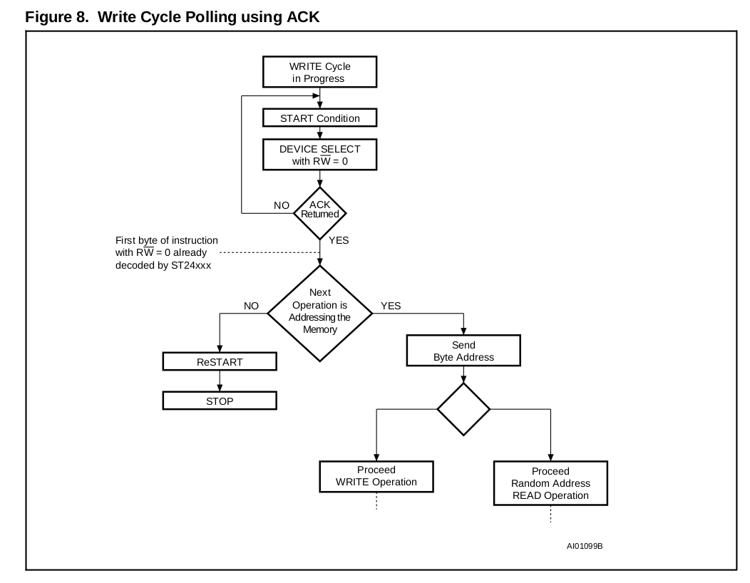 The Kernal code, instead, simply polls the SDA wire 7 times in a row with a delay between the reads of about 4.2 microseconds. This won't work if the EEPROM is busy because it would respond only once (with a NACK) and then, anyway, SDA would never change because SCL is never pulsed. At boot of course this is not a problem since the EEPROM is not busy, but in theory there could be problems afterwards. Maybe this is fixed by SetPatch or maybe the condition never happens because of how the NVRAM is accessed (I didn't analyze the code further, but from the behaviour I had observed also in other occasions, it seems that the NVRAM is re-written entirely every time StoreNV() is called, so the problem could arise only if two access requests are made almost simultaneously, which is very unlikely). Quote:
I have adjusted/improved a bit my code and also fixed a little bug: I had forgotten to send the NACK after reading the very last byte (but this wasn't the cause of the issues I reported). Now I'm waiting for other tests results. Last edited by saimo; 30 March 2020 at 23:04. |
||
|
|
|
30 March 2020, 23:12
|
#26 |
|
Registered User
Join Date: Aug 2010
Location: Italy
Posts: 787
|
The results proved my code still doesn't work: the usual variable bunch of 0s followed by all 1s.
Attached slightly revised code, whose most important change is a fix to a bug that trashed d2 (but it was not the cause of the failed tests thanks to the fact that the test address is 0). Last edited by saimo; 09 July 2021 at 09:56. |
|
|
|
05 April 2020, 13:23
|
#27 |
|
Registered User
Join Date: Aug 2010
Location: Italy
Posts: 787
|
After the previous post, I revised the code further and also made a version that accesses the registers by word (attached here); then, I prepared 2 new tests. Today I received the results, and unfortunately all they say is: 0.
In the meanwhile, my tester told me that he has a TerribleFire 330, so now I've realized what a hassle is to him to make these tests. I won't bother him anymore and I'll search for somebody who has an easier way to transfer files - by the way, anyone here? EDIT: three persons offered to help with tests, so, for the moment being, don't bother answering the help request above  Should I need further help, I'll let you know. Should I need further help, I'll let you know.
Last edited by saimo; 09 July 2021 at 09:56. |
|
|
|
05 January 2021, 16:48
|
#28 |
|
Registered User
Join Date: Aug 2010
Location: Italy
Posts: 787
|
It's quite a long time since I last worked on this stuff - I got distracted by a couple of other Amiga things (I made the demo THE CURE and the graphics system ALS) and by this programming guide (in Italian)
 - but finally I have resumed work on this! - but finally I have resumed work on this!Having almost totally forgotten how the NVRAM and my code works, I studied the datasheet and my code again, and, remembering how the Kernel code always accesses both the Akiko registers at the same time, I decided to rewrite my code entirely according to that logic (although that's a bit more inefficient). Also, I seized the chance to change the way I send the clock signal. The result is the code attached here. The good news is that this one not only works on WinUAE, but also on real Amiga CD32 machines! A tester tried it on two different machines and it was able to: dump the contents of the whole NVRAMs correctly; save data to an OS-legal entry correctly. Now I'm waiting for more test results from another friend. I still can't say that the code works 100% fine because, from the pictures on the net, I have noticed that the Amiga CD32 boards mount different versions of the chips (there are 5 V chip and chips that require a lower voltage but have slower timings) and I don't know (yet) which chips mount the machines that the tests have been performed on. Last edited by saimo; 04 September 2021 at 10:51. Reason: Removed attachment (I'm reworking the code). |
|
|
|
28 January 2021, 15:25
|
#29 |
|
Registered User
Join Date: Aug 2010
Location: Italy
Posts: 787
|
The code worked perfectly on two machines, both mounting 5V EEPROMs, with and without TF328 accelerator board. However, the game didn't fully work on a third machine with an unknown EEPROM chip and a TF300 accelerator. Unfortunately, life got in the way of my tester, so further tests remained pending for a couple of weeks. Does anybody here feel like running a few tests for me? An Amiga CD32 with a <= 2.5 V EEPROM chip and easy storage support (HD/CF/floppy/etc.) is needed.
|
|
|
|
11 February 2021, 19:38
|
#30 |
|
WinUAE developer
Join Date: Aug 2001
Location: Hämeenlinna/Finland
Age: 49
Posts: 26,505
|
Probably not much help but today I did some real I2C stuff (I2C IR temperature sensor MLX90614). Datasheet says it supports bus transfer rates from 10KHz to 100KHz. Except if it is less than about 20KHz, it failed to work every time (I think it NACKs the transfer for some unknown reason). 30KHz to 100KHz worked fine.
It also had another undocumented feature, mid transfer STOP/START condition state is not supported. If it sees STOP, it seems to reset its internal state. Only STARTs are accepted ("Repeated START"). Apparently some old EEPROMs have same limitation. So don't trust datasheets 100%.. Perhaps one possible reason is "clock stretching". Device will report NACK if host changes either line state during clock stretching. Only way to be sure is to use some logic analyzer that has I2C decoding support. Perhaps someday I'll bother with that 
|
|
|
|
11 February 2021, 23:17
|
#31 |
|
This cat is no more
Join Date: Dec 2004
Location: FRANCE
Age: 52
Posts: 8,163
|
@Saimo great work. I'd be delighted if you wrote a low-level CDTV sector read now
|
|
|
|
12 February 2021, 14:25
|
#32 |
|
Registered User
Join Date: Aug 2010
Location: Italy
Posts: 787
|
@Toni Wilen
It might be, but before assuming that there's a discrepancy between datasheet and chip, I want to be really sure that my code complies with what the datasheet says. I think it should, but the last test seems to say otherwise. But now I realize I forgot to report the full results. It goes like this... First, tests were made on the two machines that eventually proved that everything worked fine. I started with some little test proggies (among which the one that dumps the whole contents of the NVRAM, as mentioned above). Then, after getting positive results, I had SkillGrid tested (which is ultimately why I'm doing this), and, as said, it worked flawlessly. Then, the game was tried on the machine with the unknown NVRAM chip: it failed to boot, at least when running from CD. When booting, the game first makes sure that a slot is properly allocated with nonvolatile.library and then, after switching the OS off, uses the custom code to see where exactly that slot is. My guess is that this last operation fails. Now, that is done by simply dumping the whole NVRAM to a RAM buffer and I can't see why that should fail given that... the proggie that dumps the NVRAM (and that uses the same code, of course) works perfectly also on that very same machine! So, I'm suspecting that, although very unlikely, I might have broken something else in the SkillGrid startup code; on the other hand, if it were so, how can it be that the game runs on the other machines? I won't know until I get more test results. And that's the biggest issue: since I don't have an Amiga CD32, I have to rely on others. The guy who helps me with tests (a great chap, by the way) is busy with real life (well, like all of us), so at times I get a report or two after weeks or even months. When I go back to this matter I can't even remember where I was  Final outcome: the SkillGrid update has been on hold for about 1 year because of just this issue. @jotd Thank you. Now, if it only also worked...  As for the CDTV, I'm afraid I have to disappoint you: I don't really enjoy this sort of things, I'm no tech junkie... I just want to make games, and if I'm doing this is because the SkillGrid update I have here needs more RAM than before, and the only option I have to have it running on the Amiga CD32 is to trash the OS.
|
|
|
|
07 September 2021, 23:07
|
#33 |
|
Registered User
Join Date: Aug 2010
Location: Italy
Posts: 787
|
I finally returned to this.
I have rewritten the routines once again, and I have no idea of what happens on real machines. Therefore, I have prepared a proper test suite to have the routines tested... by anyone who feels like giving it a go on a real Amiga CD³² Any feedback will be much appreciated!The test suite can be downloaded from https://www.retream.com/_temporary/NVRAMRTS.lha. This short video shows what the test suite does: [ Show youtube player ] (Note: the operations will be surely slower on real machines.) Code:
--------------------------------------------------------------------------------
OVERVIEW

This is a test suite that purposes to verify whether my custom routines for
direct access to the Amiga CD³² NVRAM work.
Developing them is quite challenging because:
 · I do not have an Amiga CD³², so I have to rely on emulation, which is not
   100% exact;
 · different machines mount different EEPROM chips, which behave differently;
 · there is no official documentation (my references are the documentation that
   has been thankfully produced by who studied the behaviour of Akiko and the
   EEPROM datasheet from ATMEL, the maker of the EEPROM).
The routines work perfectly under emulation, but that is no guarantee that they
work also on real machines. Indeed, previous versions worked under emulation and
on a couple of machines, but failed on another machine.


--------------------------------------------------------------------------------
WHAT DOES THIS DO?

This suite will perform several read/write operations from/to the NVRAM, whose
DATA WILL THUS BE ALTERED (unless the routines fail to access the NVRAM
altogether). At the end, it will attempt to restore the NVRAM data exactly as it
was at the beginning.
Given that the routines are experimental, though, first it will check if a
backup of the NVRAM items exists and ask you whether to make a (new) backup, so
that the NVRAM items can be restored after the tests if the custom restore does
not succeed or execute at all (only OS-compliant NVRAM items will be backed up;
the backup and restore operations are done by means of the OS-legal, reliable,
third-party tools DumpNVRAM and RestoreNVRAM - check out NVRAM_Tools.doc).
You will be informed about the backup status and asked what to do and whether to
continue.


--------------------------------------------------------------------------------
REQUIREMENTS

· An Amiga CD³² with a writable media drive (DO NOT TRY ON OTHER MACHINES)
· The AmigaDOS Copy, Delete and Execute commands in the commands path.


--------------------------------------------------------------------------------
INSTRUCTIONS

To perform the tests:
 1. copy the NVRAMRTS directory from the archive to anywhere on the drive;
 2. from shell, enter the NVRAMRTS directory;
 3. run the "test" script and follow the on-screen instructions.

At the end of the tests or if the tests hung:
 1. reboot the machine;
 2. if the NVRAM data is not restored correctly or you are not sure, and a
    backup exists:
     2.1. from shell, enter the NVRAMRTS directory;
     2.2. run the "restore" script;
 3. pack the NVRAMRTS directory into an archive;
 4. send your Amiga CD³²'s specifications(*), the archive and, if the tests
    hung, the color of the screen at that point to postmaster@retream.com.

(*)The marking on the EEPROM would be particularly helpful, but, since that
requires opening the machine, do not worry if you do not feel like going that
far.

Thank you!


--------------------------------------------------------------------------------
THE CORE TOOL

The tests are performed by means of a tool called WriteReadNVRAM. It is a shell
program that allows to access any arbitrary chunk of the Amiga CD³² NVRAM.
It works as follows:
 1. if requested, it writes some data from an input file to the NVRAM;
 2. if requested, it saves some data from NVRAM to an output file.

The shell arguments are:
 · INPUTFILE=IF/K     : input file (unspecified = do not write data to NVRAM)
 · WRITEADDRESS=WA/K/N: NVRAM address in [0, 1023] to start writing from
 · WRITESIZE=WS/K/N   : number of bytes in [1, 1024-WRITEADDRESS] to write
 · OUTPUTFILE=OF/K    : output file (unspecified = do not read data from NVRAM)
 · READADDRESS=RA/K/N : NVRAM address in [0, 1023] to start reading from
 · READSIZE=RS/K/N    : number of bytes in [1, 1024-READADDRESS] to read
 · QUIET/S            : do not print any information to the standard output

These values are used for unspecified arguments:
 · WRITEADDRESS: 0
 · WRITESIZE   : 1024
 · READADDRESS : 0
 · READSIZE    : 1024

These values are used for invalid arguments:
 · WRITEADDRESS: 0
 · WRITESIZE   : 1024-WRITEADDRESS
 · READADDRESS : 0
 · READSIZE    : 1024-READADDRESS

If QUIET is not specified, the following information gets printed:
 · startup code : <NVRAM startup code (see below)>
 · input file   : <input file path, if specified>
 · write address: <(corrected) NVRAM address for writing>
 · write size   : <(corrected) number of bytes for writing>
 · load code    : <load code (see below)>
 · output file  : <output file path, if specified>
 · read address : <(corrected) NVRAM address for reading>
 · read size    : <(corrected) number of bytes for reading>
 · save code    : <save code (see below)>
 · elapsed time : <elapsed time expressed in color clocks>

Operation code:
 :| = no operation
 :( = operation failed
 :) = operation succeeded

No data is written to the NVRAM if loading fails.
No data is read from the NVRAM and saved to file if the NVRAM startup fails.

During execution, AmigaOS is disabled entirely. Also, the screen gets blanked
and repainted dynamically as follows:
 · blue : writing;
 · cyan : preparing to read;
 · green: reading;
 · red  : starting an operation.

THIS TOOL IS BASED ON THE CUSTOM ROUTINES WHOSE VALIDITY IS TO BE VERIFIED WITH
THIS SUITE, SO IT IS BY NO MEANS RELIABLE.
Last edited by saimo; 10 September 2021 at 21:46. Reason: Improved test script and documentation |
|
|
|
08 September 2021, 19:25
|
#34 |
|
WinUAE developer
Join Date: Aug 2001
Location: Hämeenlinna/Finland
Age: 49
Posts: 26,505
|
I can run the test this weekend (using floppy adapter)
I also have new logic analyzer (DSLogic U32Pro32) and scope (Siglent SDS2104X+) which both supports I2C decoding which should make it easy to see if there are any protocol errors. I'd like to have some explanation why some methods that you tried didn't work (but should have worked at least in theory) But I am not sure if there is any easily accessible location to connect/solder required wires.. |
|
|
|
08 September 2021, 22:48
|
#35 | |||
|
Registered User
Join Date: Aug 2010
Location: Italy
Posts: 787
|
Quote:
Quote:
Another thing I changed is SCL handling: at some point I had SCL preset to low (a bit difficult to explain in few words: basically, I was anticipating the first half of the clock), but I don't think it was a good idea (yet, if I remember correctly, that did work on some machines). Quote:
Check this picture out.
|
|||
|
|
|
10 September 2021, 21:02
|
#36 |
|
Registered User
Join Date: Aug 2010
Location: Italy
Posts: 787
|
The friend who has the machine where my routines never worked managed to give the suite a spin. And the (unsurprising result) was that the very first test hangs right at the beginning (black screen and complete freeze).
I suspect that what fails is the acknoweldge polling: for some reason, SDA always reads high, and so the code ends up looping endlessly. In theory, I could break the loop after 10 ms (that's the internal write time of the EEPROM), but that wouldn't solve the problem: the solution is understanding why SDA always reads high and fixing that. That is, or finding the actual problem, it's different. I have uploaded a new test suite (the link is always the same). The new test tool includes these changes: * at the very beginning (nvm_initialize()), SCL and SDA are first read and, if they are not both high (i.e. the EEPROM is stuck doing something), a reset procedure is executed (more about this below); * if the reset procedure doesn't work, nvm_initialize() returns error (so the test program knows that the EEPROM cannot be used); * to understand where the code hangs, the screen color gets changed dynamically as follows: green = writing; cyan = preparing to read; blue = reading; red = starting an operation (my money is on red). I tried to look at the log produced by WinUAE to see if the code behaves correctly, and something strange seems to happen. This is what happens when "number" starts to get written at address 1010 (the stuff after "<-" are my comments, which indicate the exact piece of code that executes the action): Code:
Direction write: 00->c0 <- n_initialize I2C START Data write: c0->80 (80) <- n_WriteBytes StartWrite StartOperation PullSDALow Data write: 80->00 (00) <- n_WriteBytes StartWrite StartOperation SendByte PullSCLLow Data write: 00->40 (40) <- n_WriteBytes StartWrite StartOperation SendByte SendBit (1) Data write: 40->c0 (c0) <- n_WriteBytes StartWrite StartOperation SendByte SendBit PullSCLHigh Data write: c0->40 (40) <- n_WriteBytes StartWrite StartOperation SendByte PullSCLLow Data write: 40->00 (00) <- n_WriteBytes StartWrite StartOperation SendByte SendBit (0) Data write: 00->80 (80) <- n_WriteBytes StartWrite StartOperation SendByte SendBit PullSCLHigh Data write: 80->00 (00) <- n_WriteBytes StartWrite StartOperation SendByte PullSCLLow Data write: 00->40 (40) <- n_WriteBytes StartWrite StartOperation SendByte SendBit (1) Data write: 40->c0 (c0) <- n_WriteBytes StartWrite StartOperation SendByte SendBit PullSCLHigh Data write: c0->40 (40) <- n_WriteBytes StartWrite StartOperation SendByte PullSCLLow Data write: 40->00 (00) <- n_WriteBytes StartWrite StartOperation SendByte SendBit (0) Data write: 00->80 (80) <- n_WriteBytes StartWrite StartOperation SendByte SendBit PullSCLHigh Data write: 80->00 (00) <- n_WriteBytes StartWrite StartOperation SendByte PullSCLLow Data write: 00->00 (00) <- n_WriteBytes StartWrite StartOperation SendByte SendBit (0) Data write: 00->80 (80) <- n_WriteBytes StartWrite StartOperation SendByte SendBit PullSCLHigh Data write: 80->00 (00) <- n_WriteBytes StartWrite StartOperation SendByte PullSCLLow Data write: 00->40 (40) <- n_WriteBytes StartWrite StartOperation SendByte SendBit (1) Data write: 40->c0 (c0) <- n_WriteBytes StartWrite StartOperation SendByte SendBit PullSCLHigh Data write: c0->40 (40) <- n_WriteBytes StartWrite StartOperation SendByte PullSCLLow Data write: 40->40 (40) <- n_WriteBytes StartWrite StartOperation SendByte SendBit (1) Data write: 40->c0 (c0) <- n_WriteBytes StartWrite StartOperation SendByte SendBit PullSCLHigh Data write: c0->40 (40) <- n_WriteBytes StartWrite StartOperation SendByte PullSCLLow Data write: 40->00 (00) <- n_WriteBytes StartWrite StartOperation SendByte SendBit (0) Data write: 00->80 (80) <- n_WriteBytes StartWrite StartOperation SendByte SendBit PullSCLHigh Direction write: c0->80 <- n_WriteBytes StartWrite StartOperation SendByte move.w NVMR_SCL,(a3) ;make SDA input Data write: 80->00 (40) <- n_WriteBytes StartWrite StartOperation SendByte PullSCLLow (40? NACK?) I2C device address 0xa6 <- OK Data write: 40->80 (c0) <- n_WriteBytes StartWrite StartOperation SendByte PullSCLHigh Data read: 00 <- n_WriteBytes StartWrite StartOperation SendByte or.w (a2),d2 ;read SDA (ACK/NACK) OK Direction write: 80->c0 <- move.w NVMR_SCLSDA,(a3) ;make SDA output However, right after that, the log reports that the device address $a6 has been transmitted (which is correct) and then, after I complete the 9th cycle, SDA goes low again (although SDA is supposed to change only when SCL is low) and finally the ACK is received. Maybe it's just matter of granularity of the log. But I wonder: is that (temporary) NACK supposed to simulate the fact that the EEPROM always starts with NACK and then corrects it, if needed? It looks unlikely to me, as that would equal to emulating the internal behaviour (which isn't even documented in the datasheet anyway). But then, where does that NACK come from? Additional note: if my code hadn't been able to read SDA correctly in general, it wouldn't have been also to read the contents of the NVRAM, but that is not the case; and, after all, all there is to it is pull SCL low -> wait long enough -> pull SCL high -> wait long enough -> read SDA. About the reset procedure... I have followed what the datasheet says, i.e. Code:
MEMORY RESET: After an interruption in protocol, power loss or system reset, any 2-wire part can be reset by follow-ing these steps: 1. Clock up to 9 cycles. 2. Look for SDA high in each cycle while SCL is high. 3. Create a start condition. Updated code attached here. Closing note: last week, the same friend gave the latest version of SkillGrid (which included the newly rewritten NVRAM routines) a go; as usual, the game froze at startup; but then he discovered one thing: if he booted the game without the CF card connected to the TF330, the game started up just fine (although it didn't neither read nor save to NVRAM)! Go figure... Edit: my friend just ran the latest test suite, and the result was... RED! Last edited by saimo; 04 March 2022 at 16:10. Reason: Removed attachment as I attached an updated version in a later post. |
|
|
|
12 September 2021, 12:31
|
#37 |
|
WinUAE developer
Join Date: Aug 2001
Location: Hämeenlinna/Finland
Age: 49
Posts: 26,505
|
Tested on unexpended CD32 + fWSI expansion using its internal floppy drive. No HD.
Not much happened: first some red flashing and then it hung, red screen. I'll connect probes to SDA and SCL pins later (not sure if today). Two resistors next to the EEPROM chip are SDA/SCL pullups which makes connection easy. |
|
|
|
12 September 2021, 16:47
|
#38 | ||
|
Registered User
Join Date: Aug 2010
Location: Italy
Posts: 787
|
Quote:
Quote:
|
||
|
|
|
19 September 2021, 17:31
|
#39 |
|
old bearded fool
Join Date: Jan 2010
Location: Bangkok
Age: 56
Posts: 775
|
I took a peek at nonvolatile.library, still trying to figure out what's going on in general, but thought it would be worth mentioning they always call Disable() (disabling interrupts) before doing something and Enable() when it's done.
Checking saimo's test code it looks like it relies on interrupts (CIA) to get proper timing. |
|
|
|
19 September 2021, 20:26
|
#40 | |
|
Registered User
Join Date: Aug 2010
Location: Italy
Posts: 787
|
@modrobert
Thanks for the time and the effort! Quote:
And, yes, my routines are used exclusively when the OS is off (that's the whole point: I need the routines precisely because the OS is off/trashed)
|
|
|
|
| Currently Active Users Viewing This Thread: 1 (0 members and 1 guests) | |
| Thread Tools | |
 Similar Threads
|
||||
| Thread | Thread Starter | Forum | Replies | Last Post |
| Extend CD32 NVRAM? | Amiga1992 | Hardware mods | 41 | 16 December 2018 14:59 |
| CD32 NVRAM management | Amiga1992 | support.Hardware | 9 | 20 February 2012 13:27 |
| Access CD32-NVRam from Shell | Retro1234 | support.Other | 3 | 08 August 2010 11:50 |
| CD32 nvram file...? | Christian | support.WinUAE | 11 | 13 December 2006 22:25 |
| Cd32 Nvram | Phantomz | request.Apps | 5 | 16 March 2003 21:09 |
|
|


