
|
 01 December 2019, 20:42
|
#1 |
|
Registered User
Join Date: Aug 2019
Location: The Netherlands
Posts: 115
|
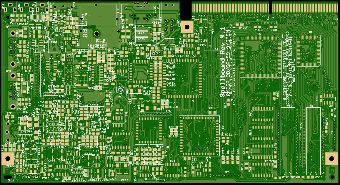 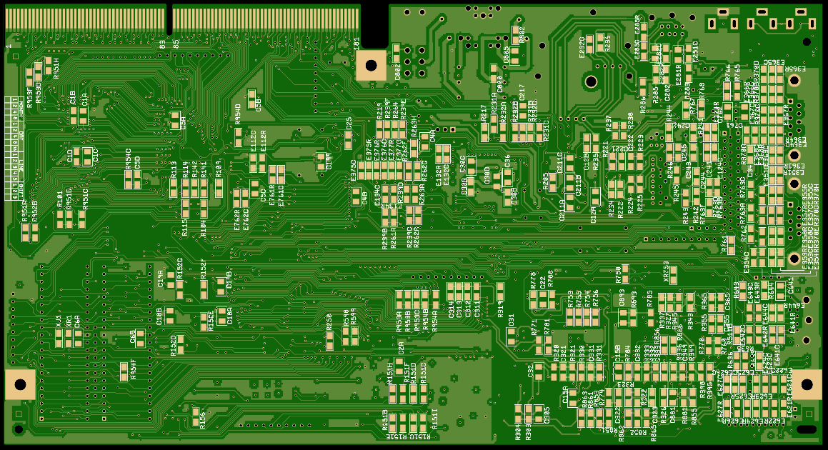 Amiga CD32 Rev4.1 Gerber files converted from SVG data at amigapcb.org GitHub repository with Sprint Layout file and Gerber files: I have removed this link and after discussing with CD32Freak - BippyM Feedback is welcome! :-) Edit 2019-12-11: I've made a mistake with the Sprint Layout Gerber export and updated the files in the repository. 2019-12-13: Updated images of top and bottom 2019-12-25: Fixed some minor pad errors Last edited by BippyM; 31 July 2020 at 19:31. |

|
|
01 December 2019, 21:17
|
#2 |
|
Registered User
Join Date: Jan 2004
Location: Yorkshire
Posts: 710
|
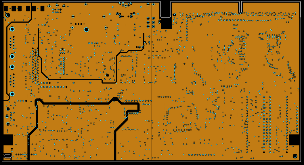
From what I've read ground plane should be layer 2 closest to logic and layer 3 vcc.
If you're asking what those light green traces are the long zigzaggy trace along the top and wide vertical one on the left looks like the analogue (audio) ground, on the A600 and A1200 pin 37 of Paula isn't connected directly to ground but is connected to a bunch of other things and has a shared ground at the audio connectors. A couple of the thin traces above it are for left and right audio channel which have pins on the expansion connectors, presumably for audio input/output for expansion cards? the u shaped one on the right and the horizontal one at the bottom looks like part of the +12V. Could it just be because the AmigaPCB 4.1 is still beta? or could the 4.1 board have actually been 6 layer? edit: it looks like the CD32 has 2 left and 2 right (internal and external) signals going to the expansion connector so that's what the 4 little traces are. Ideally you would probably want the audio stuff on the ground layer. +12V where ever it fits? Last edited by Mick; 01 December 2019 at 21:34. |
|
|
|
03 December 2019, 13:40
|
#3 |
|
Registered User
Join Date: Aug 2019
Location: The Netherlands
Posts: 115
|
Thanks Mick. I think I've converted the GND layer wrong, now it doesn't make sense. What black is should be copper en what orange is should not be copper. What do you think?

|
|
|
|
03 December 2019, 13:56
|
#4 |
|
Registered User
Join Date: Jan 2004
Location: Yorkshire
Posts: 710
|
Does the walled off area on the bottom connect to the walled off area on the left via a thick trace?
I'm only going by what I've learned in the last 6 months or so but it looks to me like they've partitioned the ground plane to keep digital noise out of the analogue ground areas, the walled off area on the bottom is audio components and I'd guess that it connects to the walled off area on the left and then connects to the normal (digital) ground at the audio connectors, the video components area has a u shaped wall around it so that digital noise won't go through and pollute the video components' analogue ground area. On my A1200 design I've struggled to auto route it to 4 layers so I've done it 6 layers and I have two different ground layers, one for analogue and one for digital. Last edited by Mick; 03 December 2019 at 15:02. |
|
|
|
03 December 2019, 16:32
|
#5 |
|
Registered User
Join Date: Aug 2019
Location: The Netherlands
Posts: 115
|
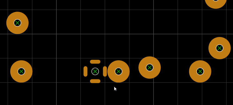
Yes, the board is surrounded with a thick trace. I thought a ground plane should cover the whole layer, because the individual vias have only a circle around them and aren't connected to anything:
 It seems to me I should use the VCC and the OVV layers: 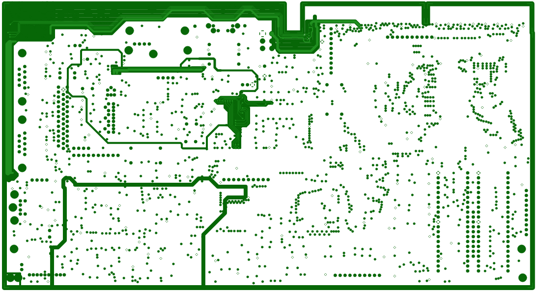
Last edited by CD32Freak; 03 December 2019 at 17:30. |
|
|
|
03 December 2019, 18:55
|
#6 |
|
Registered User
Join Date: Jan 2004
Location: Yorkshire
Posts: 710
|
What is on each of the 3 internal layers? can you post separate screenshots? it sounds to me like it would be easier to learn KiCad.

Last edited by Mick; 03 December 2019 at 19:00. |
|
|
|
04 December 2019, 11:34
|
#7 |
|
Registered User
Join Date: Aug 2019
Location: The Netherlands
Posts: 115
|
Are you kidding? When I started KiCad for the first time, I wanted to rename the weird default layer names, for example F.Cu (Front Copper layer), but then I discovered you can't! The developers must be so stubborn not to even give you the option
") I'm impressed that you've designed the A600 with KiCad I'm impressed that you've designed the A600 with KiCad  Anyway, here are the 3 inner layers from amigapcb.org OVV 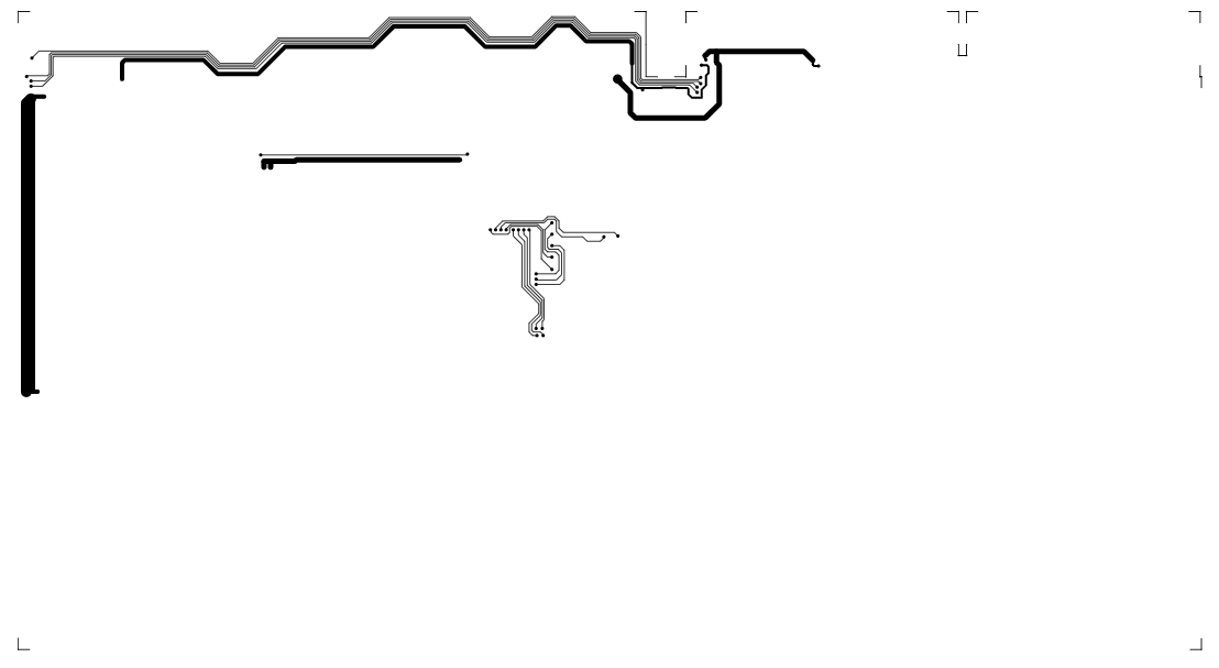 VCC 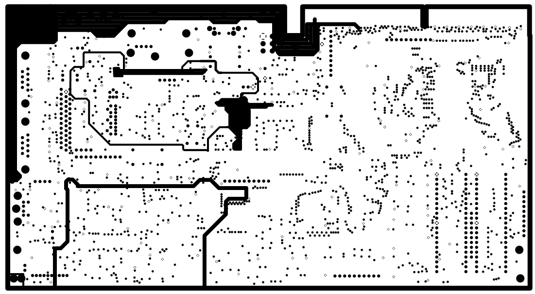 GND 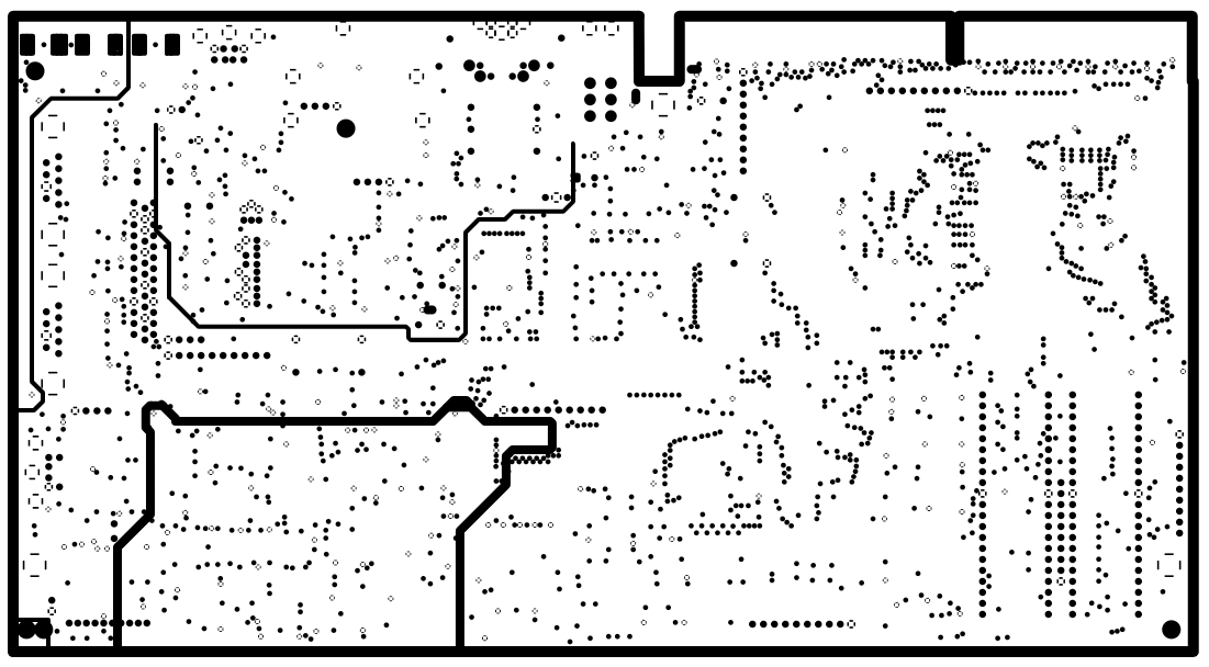
|
|
|
|
04 December 2019, 12:13
|
#8 |
|
Registered User
Join Date: Jan 2004
Location: Yorkshire
Posts: 710
|
Looking at that I would think that VCC and OVV go on the same layer?
|
|
|
|
04 December 2019, 15:02
|
#9 |
|
ex. demoscener "Bigmama"
Join Date: Jun 2012
Location: Fyn / Denmark
Posts: 1,624
|
Yes, it indeed looks like the traces for VCC and OVV belong on the same layer - maybe they were separated in the pcb explorer to make it clearer, that they are different voltages?
@cd32freak: you can indeed rename layers in Kicad, at least in the V5.1 I'm using at the moment :-) |
|
|
|
04 December 2019, 16:00
|
#10 |
|
Registered User
Join Date: Jan 2004
Location: Yorkshire
Posts: 710
|
It might be because it's a mixed layer so the plane and traces are separated in the software.
|
|
|
|
04 December 2019, 16:58
|
#11 |
|
Registered User
Join Date: Aug 2019
Location: The Netherlands
Posts: 115
|
Thanks hooverphonique and Mick, but it seems to me there are important tracks on OVV that should be separated and not mixed with one thick track on VCC. Very confusing
 @hooverphonique You can only change the name of F.Cu and B.Cu in the Board Setup, that doesn't count. I want to right-click a layer and select edit layer or something 
Last edited by CD32Freak; 04 December 2019 at 17:15. |
|
|
|
04 December 2019, 17:35
|
#12 | ||
|
ex. demoscener "Bigmama"
Join Date: Jun 2012
Location: Fyn / Denmark
Posts: 1,624
|
Quote:
Quote:
|
||
|
|
|
04 December 2019, 18:01
|
#13 |
|
Registered User
Join Date: Jan 2004
Location: Yorkshire
Posts: 710
|
Like hooverphonique says the black areas on the VCC layer are no copper areas so the traces should slot in nicely. I'd assume it's possible to merge them both somehow?
What colour do the traces show as on the outer layers? if the planes/traces are inverted then that might be why they're stored separately. Last edited by Mick; 04 December 2019 at 18:12. |
|
|
|
05 December 2019, 11:15
|
#14 |
|
Registered User
Join Date: Aug 2019
Location: The Netherlands
Posts: 115
|
Yes, that's what I wrote earlier
The dark areas are the original SVG objects I've made black in de css file to be converted into Gerber format. I also thought the light green areas should be copper, but that's not how it's created with SVG objects at amigapcb.org webpage. Here is an image from amigapcb.org where you can see the VCC and OVV layers together. The GND layer is default hidden and you can only see it if you press F12 in Chrome and change the visibility to visible instead of hidden: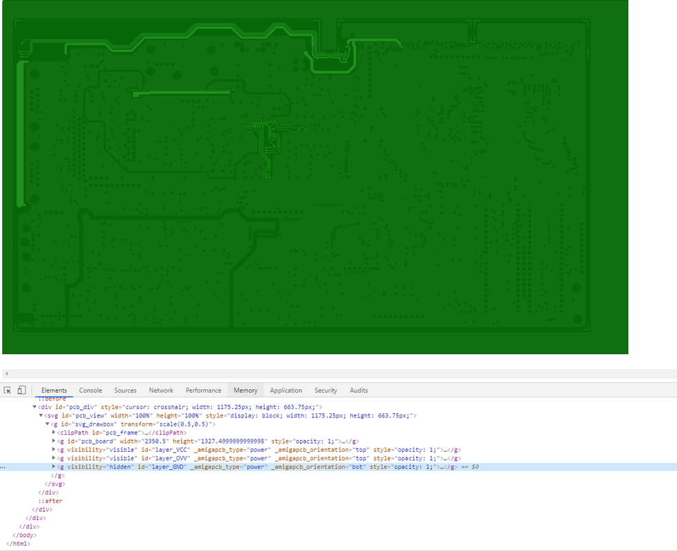
|
|
|
|
05 December 2019, 13:58
|
#15 |
|
Registered User
Join Date: Aug 2019
Location: The Netherlands
Posts: 115
|
The tool FAB3000 I'm using to convert the PDF to Gerber has an option to pour copper around everything that's black. Cool, we're getting closer
|
|
|
|
05 December 2019, 14:05
|
#16 |
|
Registered User
Join Date: Jan 2004
Location: Yorkshire
Posts: 710
|
Isn't there an option to merge the OVV and VCC files in it or is that too easy?
|
|
|
|
05 December 2019, 16:32
|
#17 |
|
Registered User
Join Date: Aug 2019
Location: The Netherlands
Posts: 115
|
I am able to pour copper around where it should be
Last edited by CD32Freak; 06 December 2019 at 17:31. |
|
|
|
13 December 2019, 15:38
|
#18 |
|
Registered User
Join Date: Aug 2019
Location: The Netherlands
Posts: 115
|
I have updated the design with adding missing holes at CN3, CN4 and CN10. After examining images of a blank rev 3 PCB at Big Book of Amiga Hardware
(https://www.bigbookofamigahardware.c...uct.aspx?id=32) I come to the conclusion that the VCC layer at amigapcb.org is not used at all on an original CD32 board. Only the GND en OVV layers are used. |
|
|
|
17 December 2019, 10:26
|
#19 |
|
Registered User
Join Date: Aug 2019
Location: The Netherlands
Posts: 115
|
Oh *bleep*, I see the Akiko pads have no soldermask. It seems nobody is interested in a CD32 reborn, so I will quietly update the files...hush!
|
|
|
|
17 December 2019, 22:24
|
#20 | |
|
Tech Guru
Join Date: Dec 2015
Location: Oxnard, CA
Posts: 189
|
Quote:
|
|
|
|
| Currently Active Users Viewing This Thread: 1 (0 members and 1 guests) | |
| Thread Tools | |
 Similar Threads
|
||||
| Thread | Thread Starter | Forum | Replies | Last Post |
| Amiga 2000 Rev4.4 Resistor Array types | ronybeck | support.Hardware | 2 | 14 August 2019 13:17 |
| Looking for app that allow copy files to CD32 NVRAM or mount it as disk | elder | request.Apps | 8 | 27 October 2016 13:18 |
| Playing CD32 Games that have Wav files Included? | Kitty | New to Emulation or Amiga scene | 4 | 04 October 2009 11:55 |
| Gerber files | Kristian95 | Hardware mods | 19 | 14 June 2008 19:33 |
| Burning CD32 files + (mp3) audio | kriz | Retrogaming General Discussion | 5 | 25 November 2003 13:49 |
|
|


