
|
 22 February 2020, 15:27
|
#21 |
|
Registered User
Join Date: Sep 2019
Location: Redcar, UK
Posts: 42
|
Oh i didn't realise that it's just i have an a600 but the motherboard is completely shot (it has a hole in it where it caught fire) just thought this would have been a good way to keep it alive so to speak.
If i manage to work out how to use the gerber files to produce a working board i'll let you know |

|
|
22 February 2020, 15:31
|
#22 | |
|
Registered User
Join Date: May 2018
Location: Germany, Baden-Wuerttemberg
Posts: 387
|
Quote:
|
|
|
|
|
22 February 2020, 15:38
|
#23 |
|
Registered User
Join Date: Sep 2019
Location: Redcar, UK
Posts: 42
|
No i hadn't seen that thread it's rather helpful thanks for letting me know
|
|
|
|
22 February 2020, 22:01
|
#24 |
|
Registered User
Join Date: Jan 2004
Location: Yorkshire
Posts: 710
|
I've pretty much done the A1200, going to make a start on A600 next week trying to decide if I should include the planes as I can always remove them later if they aren't necessary? rather over engineer a board than be left head scratching again.
|
|
|
|
23 February 2020, 00:03
|
#25 |
|
Registered User
Join Date: Sep 2019
Location: Redcar, UK
Posts: 42
|
Will you be selling the boards for the a600 when you have done it ? or sharing the gerber files?
|
|
|
|
24 February 2020, 13:24
|
#26 |
|
Registered User
Join Date: Jan 2004
Location: Yorkshire
Posts: 710
|
I was just going to release the files for a basic design (original board + CXA2075 mod listed here and S-Video at this point), I'm not looking to make money or wave it around telling everybody I can't share for x reason. TBH it all just started as me playing around Kicad and all I want is a basic/original/minimalist A1200 board for my own use. I only started on the A600 because it looked easier to learn from and now that people want it I'm trying to get it done for everyone else so I can move on to A1200 which is my main goal. If people want to modify/improve it later then it's up to them. Let freedom reign.

Last edited by Mick; 24 February 2020 at 13:29. |
|
|
|
24 February 2020, 13:28
|
#27 |
|
Registered User
Join Date: Sep 2019
Location: Redcar, UK
Posts: 42
|
Thats great as i only want an original board for an a600 to replace one that is damaged beyond repair as i used to have one as a kid and i enjoy the nostalgia when playing it.
I actually still have the same amiga i had when i was a kid thats why im really wanting to get my hands on a new board to repair it |
|
|
|
24 February 2020, 13:32
|
#28 |
|
Registered User
Join Date: Jan 2004
Location: Yorkshire
Posts: 710
|
Yeah I think there'd be interest in just a close to original board for repairs and such but a lot of people want the Swiss army knife of boards with all sorts of mods to it which I've tried to resist doing, if someone wants to make one of those later using my files then it's fine by me.
|
|
|
|
24 February 2020, 13:54
|
#29 |
|
Registered User
Join Date: Sep 2019
Location: Redcar, UK
Posts: 42
|
I agree with you. Personally i dont think you can beat original hardware i don't go for all the mods to me it kind of defeats the point of using original hardware when you mod it.
I wish you look and look forward to seeing the finished product of your work |
|
|
|
25 February 2020, 16:37
|
#30 |
|
Registered User
Join Date: Jan 2004
Location: Yorkshire
Posts: 710
|
This 2A revision definitely seems a little bit incomplete which might be why it never saw the light of day. These are the issues I've found:
C239 not connected to ground (no via). (EDIT: nvm it is connected to ground through the modulator) The power trace below Gayle not linking up as rvctech has pointed out in my thread. 2-3 other missing VIA's that should stitch ground traces. Last edited by Mick; 26 February 2020 at 12:58. |
|
|
|
26 February 2020, 06:18
|
#31 |
|
Registered User
Join Date: Aug 2019
Location: The Netherlands
Posts: 115
|
Yes, you are right, Mick. I can see hidden GND tracks on the original TOP layer SVG data that I have saved, which should be on a seperate GND ID. Scrat has now protected his site even more by putting all layers into one ID, but when you click pin 2 of C239, you can see this hidden GND layer in the xray layer_XRT ID:
 
|
|
|
|
26 February 2020, 12:46
|
#32 |
|
Registered User
Join Date: Jan 2004
Location: Yorkshire
Posts: 710
|
I'm not following they both look the same to me but I've just checked and the missing via's are displayed on amigapcb too.
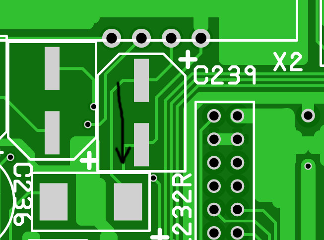   EDIT: Ahh, C239 is connected to ground through the modulator... I didn't see that as I removed it pretty early on. I think they fixed these missing via's in the 2B board though looking at a photo. Last edited by Mick; 26 February 2020 at 13:05. |
|
|
|
26 February 2020, 22:41
|
#33 | |
|
Registered User
Join Date: Dec 2018
Location: Sydney / Australia
Posts: 96
|
Quote:
Hi CD32Freak, When I did my own conversion of the SVG data to my CAD package, I saw these. They are not really "hidden" GND tracks. They are just a relic from when the PCB was designed by Commodore. The fact that they can be seen on AmigaPCB made it very obvious that the data was direct from the original Gerbers (if that was not already obvious). I did convert these special tracks too, for the sake of completeness. Also some of them increase the width of the copper pour slightly. The PCB designer would have created GND tracks to start with, to join all GND nodes. Afterwards they "poured copper" over a designated area, which covers many of these tracks. The above process is normal in the PCB design flow and I have worked with many people that do this. I also have done this. Others designers, do not do this. Instead they simply leave GND points disconnected, and in the final step, they pour copper and rely on that to join all GND nodes. When the PCB is manufactured, only the end result matters. The Gerber plotter is "double flashing" where both a track and a pour exists, in those areas, these "hidden" tracks become redundant. It's nice to treat these extra GND tracks as separate, but they mostly make no difference to the manufactured PCB when they are overlaid with poured copper. Hope this makes sense. Last edited by rvctech; 26 February 2020 at 22:59. |
|
|
|
|
26 February 2020, 23:41
|
#34 |
|
Registered User
Join Date: Jan 2004
Location: Yorkshire
Posts: 710
|
What did you do your board in rvctech? can we see it? did you find any other problems apart from the vcc trace below Gayle and the couple of missing via's I've found?
|
|
|
|
27 February 2020, 07:25
|
#35 |
|
Registered User
Join Date: Aug 2019
Location: The Netherlands
Posts: 115
|
Thanks for the explanation, rvctech, but I see GND tracks running through signal tracks. Wouldn't that mean they should be on a seperate GND layer? By the way, what CAD package did you use to convert the SVG data?
|
|
|
|
27 February 2020, 10:43
|
#36 | |
|
Registered User
Join Date: Dec 2018
Location: Sydney / Australia
Posts: 96
|
Quote:
Some of those tracks that you have highlighted are running on the bottom layer, not the top. I think the "x-ray" layer is a visualisation tool for showing where a particular net runs (across all layers). I ignored this layer when performing my conversion, as all the required layer data appears on its respective layer anyway. I have attached a screenshot from my CAD tool that shows the GND copper both on top (red) and bottom (blue) layers. You can see how it covers the GND that your "x-ray layer" has highlighted. I extracted the SVG data manually from the HTML (removed extraneous data), and I converted and scaled the SVG data with Inkscape into a DXF file. I originally wanted to convert from SVG to Gerber without the use of commercial tools that I don't own, but all the free tools that I found failed at this. I considered writing my own quick and dirty conversion tool (there is a lot of conceptual similarity between SVG and Gerber), but I was doing a proof of concept, so I left this exercise for another time, and instead exported the data to a DXF. I then imported this file directly into my ECAD package (Altium Designer). From there I converted it into a native PCB. The AmigaPCB data (and by extension the Original Commodore Gerber data) does have two additional internal plane layers (GND, VCC) but these are just planes, there are no tracks. I would guess that Commodore ultimately decided to manufacture as a 2-layer board to save costs. |
|
|
|
|
27 February 2020, 10:54
|
#37 | |
|
Registered User
Join Date: Dec 2018
Location: Sydney / Australia
Posts: 96
|
Quote:
Hi Mick, I use Altium (my tool of the trade). In theory I can do some checks on the PCB (such as antenna tracks that lack vias) but I can't do this until I do some more work on the PCB/schematic linkage inside Altium. I've attached a screenshot of the PCB (almost complete). I haven't worked on it in a few weeks :-(. I started work on it in Dec 2019 after CD32Freak posted a teaser image of his CD32 conversion ;-). The only other thing that I found wrong so far, was that a mounting hole for the joystick connector is wrong. |
|
|
|
|
27 February 2020, 12:48
|
#38 |
|
Registered User
Join Date: Jan 2004
Location: Yorkshire
Posts: 710
|
How do you mean wrong? the way they are offset for the case?
I noticed that nearly all of the mounting holes were quite a bit off and most other things were not exactly where they should be according to data sheets. It seems like the way Commodore did it wasn't all that precise, even the edge connectors seem to have ever so slightly differing pitch in places, it's not perceivable by eye and won't make a different to use but mathematically inaccurate at least. Even their resistor footprints have slightly varying lengths, PLCC patterns aren't exactly square etc. I guess it might have been a limitation of the software back then? dunno. If you find anything let me know. 
Last edited by Mick; 27 February 2020 at 12:59. |
|
|
|
27 February 2020, 13:35
|
#39 | |
|
Registered User
Join Date: Dec 2018
Location: Sydney / Australia
Posts: 96
|
Quote:
Completely understand what you mean with respect to footprint inconsistencies. I don't know if the software was less accurate, or if people were slightly more lax back then! I converted a 1990s PCB in my day job, and every part had a slightly different pad size  . The silkscreen was all over the shop too. . The silkscreen was all over the shop too.
|
|
|
|
|
27 February 2020, 14:40
|
#40 |
|
Registered User
Join Date: Aug 2019
Location: The Netherlands
Posts: 115
|
@rvctech
The tool I'm using (FAB3000) imports PDF using Ghostscript (specifically the gsdll32.dll) and that is free, maybe that could help you further creating your own conversion tool There is also a free Perl script called pdf2gerb, but that didn't work for me: https://github.com/swannman/pdf2gerb Someone else also wrote a PDF to Gerber converter for his Minimoog replica, but he doesn't want to release the code: https://inaptlycrafted.blogspot.com/...converter.html The CD32 is the only board I fixed with Sprint-Layout and the others are direct conversions from amigapcb. It could be that the SVG data is not properly converted from the original Commodore files Scrat used 
Last edited by CD32Freak; 27 February 2020 at 14:48. |
|
|
| Currently Active Users Viewing This Thread: 1 (0 members and 1 guests) | |
| Thread Tools | |
 Similar Threads
|
||||
| Thread | Thread Starter | Forum | Replies | Last Post |
| Amiga 4000D Rev B gerber files | CD32Freak | Hardware mods | 39 | 08 October 2021 10:11 |
| Amiga CD32 Rev4.1 Gerber files | CD32Freak | Hardware mods | 47 | 16 March 2021 16:01 |
| A4000T Rev4 gerber files | CD32Freak | Hardware mods | 8 | 22 February 2020 19:51 |
| First Amiga 600 FPGA Accelerator - Vampire 600 | majsta | Hardware mods | 736 | 18 July 2016 18:31 |
| Gerber files | Kristian95 | Hardware mods | 19 | 14 June 2008 19:33 |
|
|


